Plasma is used for many different applications such as deposition or etching processes.
A huge variety of sources (DC, RF, microwave, …) leads to a high demand on universal diagnostic tools.
Thus, easily accessable parameter such as voltages or emission are measured.
All those values are indirect parameters that do no allow insights in the plasma – which is responsable for the product forming process!
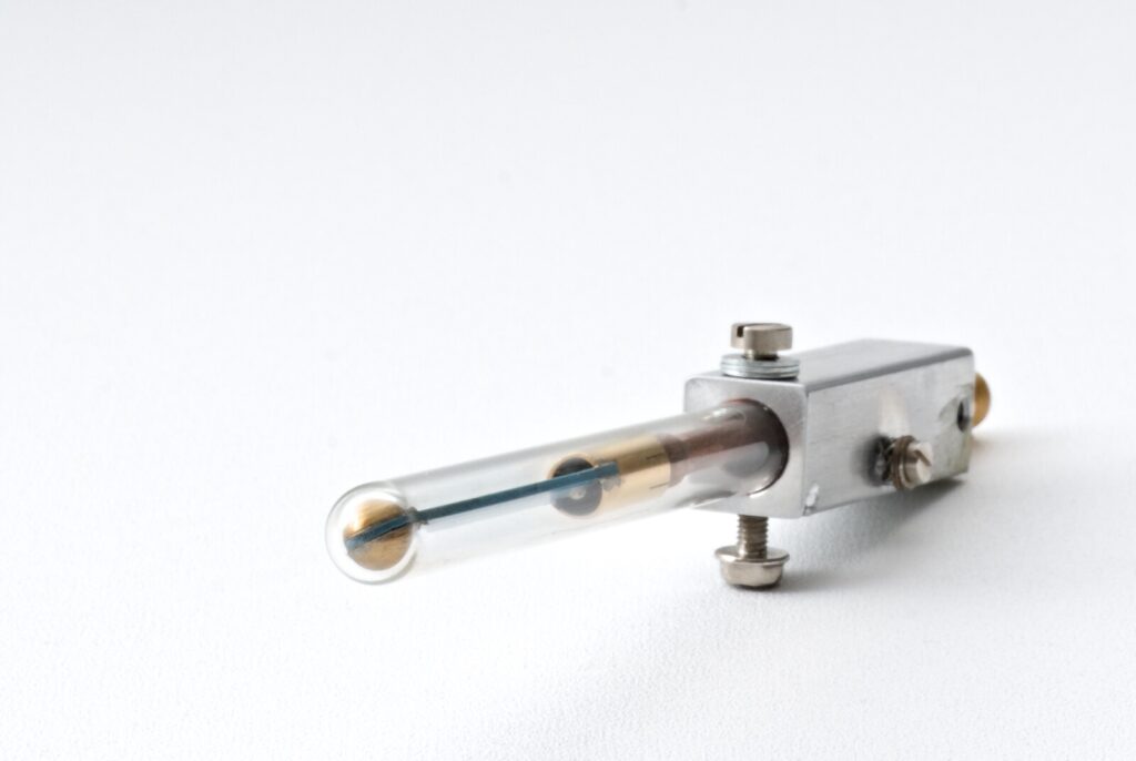
The Multipole Resonance Probe (MRP) is based on the principle of active plasma resonance spectroscopy and measures in-situ and real-time the electron density as well as the electron temperature and electron collisionfrequency – the most important plasma parameters.
Knowing these values, flows and distribution functions can be estimated.
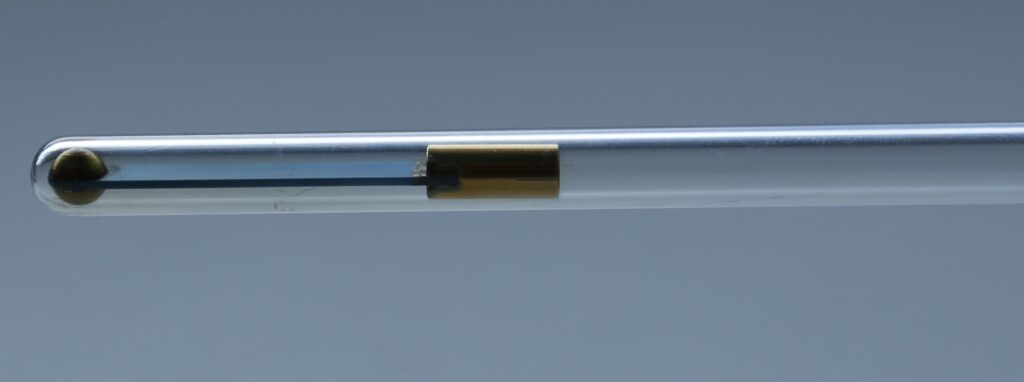
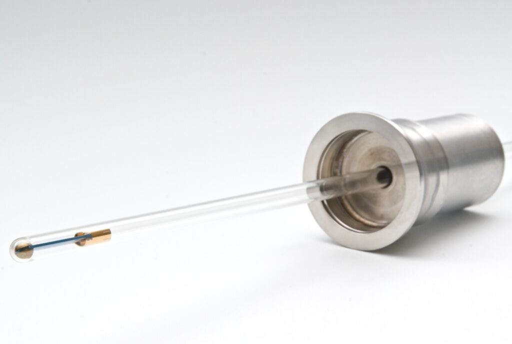
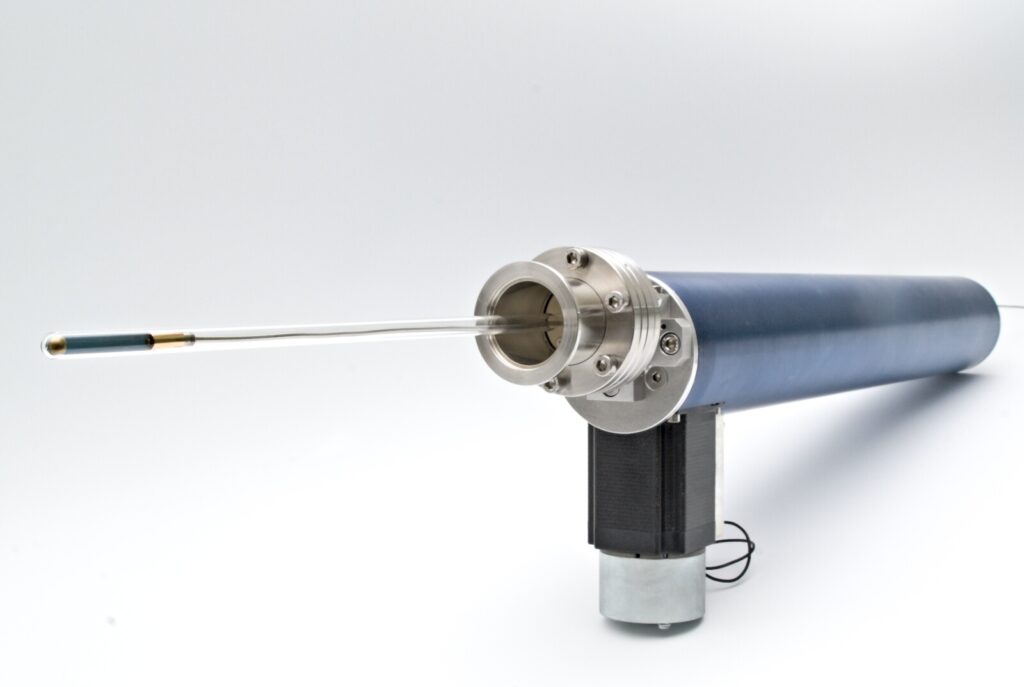
It is mounted in a ceramic tube – this makes the MRP measurement insensitive against dielectric coatings.
FITTING MARKETS
The Multipole Resonance Probe was already used in a high amount of different set-ups. It was implemented in optical deposition and other photonic systems, during glass coating as well as in etching or PECVD and HPPMS processes.
It works in capacitively or inductively coupled plasmas, with microwave sources, in dusty plasmas, with DC, MF, RF, pulsed, …
The MRP works universally in low-pressure and low-temperatureplasmas, used in photonics, glass manufacturing, semiconductor processing and many many more. There are different designs for every application.
Let’s check, if it fits to your system!
Plasma
Why is plasma needed?
Production of everyday needs use plasma technology. Pictures: Unsplash von CoWomen, Christian Bruno, Alexandre Debieve, Mariana Proenca, Steve Johnson, NASA
The deposition of thin, nanostructured layers is one of the key tasks of our modern production technology. Many everyday products, such as electronic devices, PET bottles, functional surfaces, solar cells, space technology, eyeglasses coating, lenses or large architectural glasses require such process technology. Etching and coating processes are used to structure materials on a microscopic level. This enables functional coatings to repel water, for special robustness or compatibility with biological organisms as well as decontamination of surfaces or improved gas barriers in PET bottles for product protection. The processes used are mostly plasma-assisted, technically demanding, physically and chemically complex, and offer the user a wide range at least theoretically many degrees of freedom.
“Without this technology, we would be stuck in the 1970s listening through tinny headphones to disco music on our “small” portable cassette tape player. Carrying laptops around would be more for fitness than for convenience and mobile “smart” phones would require wheels.“
Plasma etching: “Yesterday, today, and tomorrow”, Journal of Vacuum Science & Technology A 31, 050825, 2013
write Donnelly and Kornblit of the University of Houston in 2013 to emphasize the importance of plasma process technology, especially for etching applications in microsystems technology.
But what is a plasma?
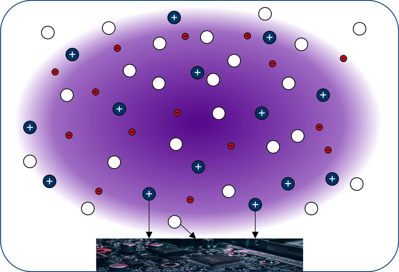
In fact, plasmas surround humans. Above all, matter in space is in the so-called plasma state, which is often defined as the fourth state of matter (besides solid, liquid and gaseous states). It describes a gas that is ionized to a certain degree. Free charged particles (electrons, ions) can be transported in fields, which defines a current. Examples of naturally occurring plasmas are for instance the sun, lightnings and northern lights. Free electrons in space, which are released from atoms or molecules by cosmic radiation, for example, are accelerated by electric fields and collide with heavy gas particles. Elastic collisions change the momentum of the particles. Inelastic collisions, on the other hand, change the internal energy of mainly heavy particles. For instance, dissociation, excitation and ionization take place. During ionization, pairs of negatively charged electrons and positive ions are formed by releasing an electron from the atomic body of the neutral particle.
Plasma with neutral particles (white), positive ions (blue +) and negative electrons (red -)
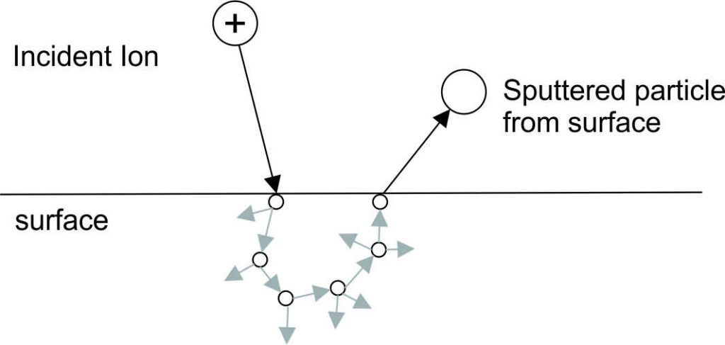
Application example: Sputter deposition
For more than 100 years, sputtering processes have been known for their use in thin film deposition. These layers are urgently needed in various fields such as the optical industry. Different sputtering technologies and a variety of measurement techniques have been developed over the centuries. Sputtering is classified as a physical vapor deposition (PVD) technique. In this process, a solid body is treated as a target by a plasma in low pressure. High energy ions, e.g. argon ions, which hit this target break surface bonds and knock single atoms out of the solid. These particles condense on surfaces, for example on a substrate. First publications on these processes date back to the 19th century. Common processes are (pulsed) direct current or medium frequency magnetron plasmas. In the 1930s, the large field of sputter coating was expanded to include roll-to-roll processes on flexible substrates. At the beginning of the second half of the 20th century with help of better models new and modern concepts for high frequency (HF) capacitively coupled plasma (CCP) were developed. Especially the use of rotating magnetrons in the early 1980s enabled a tunable asymmetrical magnetron sputtering with higher ionization efficiency and even later pulsed High-power pulsed magnetron sputtering (HPPMS).
Sputter cascade: incident ion transfers energy to the solid, an atom is sputtered from the surface
The beginning of “reactive sputtering” first appeared in 1953. By using additional reactive gas, it is possible to deposit a ceramic composite layer using a metallic target surface. For example, oxygen reacts with sputtered aluminum to form aluminum oxide. The mechanisms altered by the target oxidation, for example the secondary electron emission and the sputter yield, are still the subject of research. At least eight Nobel Prize winners in physics and chemistry had a major influence on the development of modern sputter coating, for example Joseph Thomson in 1906 for his discovery of the electron or Irving Langmuir in 1932 for his work on surface chemistry.
Multipole Resonance Probe – Function
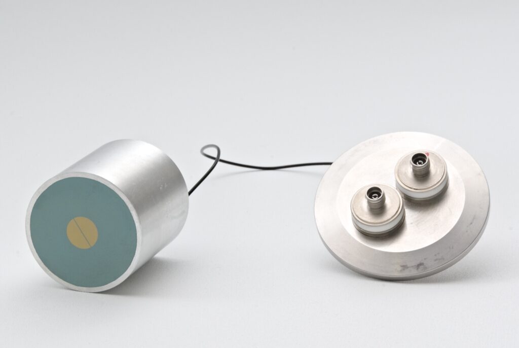
Plasma diagnostics with real-time-capable electronics and evaluation should provide insights in the plasma process . The multipole resonance probe (MRP) was developed for this purpose at the Ruhr University Bochum. It provides measurement data on ● electron density ●collision frequency, as well as ●electron temperature – the most important internal plasma parameters. The measuring time with the MRP is therefore short and, thus, the probe can be used in real-time applications. Furthermore, it provides direct plasma parameters in the evaluation in contrast to the indirect, external parameters which are often used and therefore only allow indirect control of processes. The probe is available in different hardware versions as well as with software solutions to fulfill all requirements.
The measuring principle is based on active plasma resonance spectroscopy (APRS). The probe is used to couple a high-frequency signal in the megahertz to gigahertz range via a dielectric into the plasma. At a frequency close to the electron plasma frequency, the plasma absorbs the energy of the signal and resonates. The response of the plasma-probe-system – the reflection value S11 – is picked up by the probe and transmitted to an evaluation unit. The MRP is a special realization of the APRS, which is characterized by a high geometric and electrical symmetry. The probe head consists of two symmetrically arranged electrodes designed as hemispheres, which are controlled electrically symmetrically. Due to this symmetry, the behavior of the probe can be analyzed mathematically transparent and a formulaic relationship between the resonance frequency fres and the electron density of the plasma can be specified: